- メール
- 電話
-
住所
洪山区珞獅南路147号未来城A棟
Maikono Technology Co., Ltd
概要
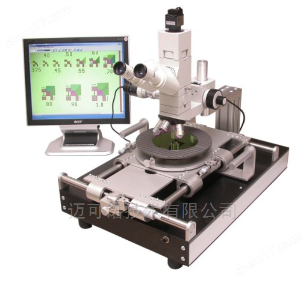
COMEFは、線幅と線距離を高精度に測定するために設計された、特殊な機能を備えた画像処理ソフトウェアです。グレースケール値アルゴリズムにより、シリコンウエハ上のワイヤまたは構造の幅と間隔をサブピクセルレベルの精度で測定することができます。
製品詳細
COMEFは、線幅と線距離を高精度に測定するために設計された、特殊な機能を備えた画像処理ソフトウェアです。グレースケール値アルゴリズムにより、シリコンウエハ上のワイヤまたは構造の幅と間隔をサブピクセルレベルの精度で測定することができます。
それは光学イメージングの可逆的な原理を応用した。そのため、CCDチップを物平面(サンプル平面)に置くことも想像できる。10倍の増幅率で試験サンプルをチップレベルに結像する顕微対物レンズは、原則として1/10の増幅率で試験サンプルレベルにチップを結像する。
サブピクセル処理とは?Subpixeling means, detection of edge position with higher reproductibility than ΔXm. How does that work?これはどのように動作していますか。A condition is that the recognition of the edge position does not take place manually any longer via setting measuring points on the PC monitor.条件としては、エッジ位置の認識は、コンピュータディスプレイに手動で測定点を設定することによって行われなくなります。The edge recognition is made on the basis of grey tone distributions by the regarded screen window. Thus this measuring procedure no more is suitable for all kinds by objects.エッジ識別は、観察されたスクリーンウィンドウのグレートーン分布に基づいて行われる。そのため、この測定方法はすべてのタイプの物体に適用されなくなった。It works however outstanding perfect for all linear expanded objects, thus e.g. for circuit paths on hoppers or structures on wafers and masks in semiconductor technology.しかし、半導体技術における回路経路、ホッパ上の構造、およびウエハおよびマスク上の構造など、すべての線形拡張物体に対して優れており、適用可能である。
チップ上の元のピクセルサイズは6マイクロメートルであるため、テストサンプルレベルでのピクセル当たりのサイズは0.6マイクロメートルである。